 Datasheet下载
- 型号: 142-0761-821
- 制造商: AIM-Cambridge/Emerson
- 库位|库存: xxxx|xxxx
- 要求:
| 数量阶梯 | 香港交货 | 国内含税 |
| +xxxx | $xxxx | ¥xxxx |
查看当月历史价格
查看今年历史价格
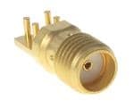
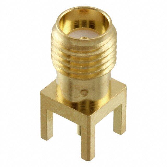
142-0761-821产品简介:
ICGOO电子元器件商城为您提供142-0761-821由AIM-Cambridge/Emerson设计生产,在icgoo商城现货销售,并且可以通过原厂、代理商等渠道进行代购。 142-0761-821价格参考¥43.83-¥75.13。AIM-Cambridge/Emerson142-0761-821封装/规格:同轴连接器(RF), 板边缘,末端突出式,通孔,直角 SMA 连接器 插孔,母形插口 50 欧姆 焊接。您可以下载142-0761-821参考资料、Datasheet数据手册功能说明书,资料中有142-0761-821 详细功能的应用电路图电压和使用方法及教程。
| 参数 | 数值 |
| 产品目录 | |
| 描述 | CONN SMA JACK 50 OHM EDGE MNTRF连接器/同轴连接器 PCB JACK 50 OHM GOLD ROUND BODY |
| 产品分类 | 同轴连接器 (RF)射频互连 |
| 品牌 | Emerson Network Power Connectivity JohnsonJohnson / Emerson Connectivity Solutions |
| 产品手册 | http://emersonconnectivity.com/OA_HTML/ibeCCtpItmDspRte.jsp?item=4253600 |
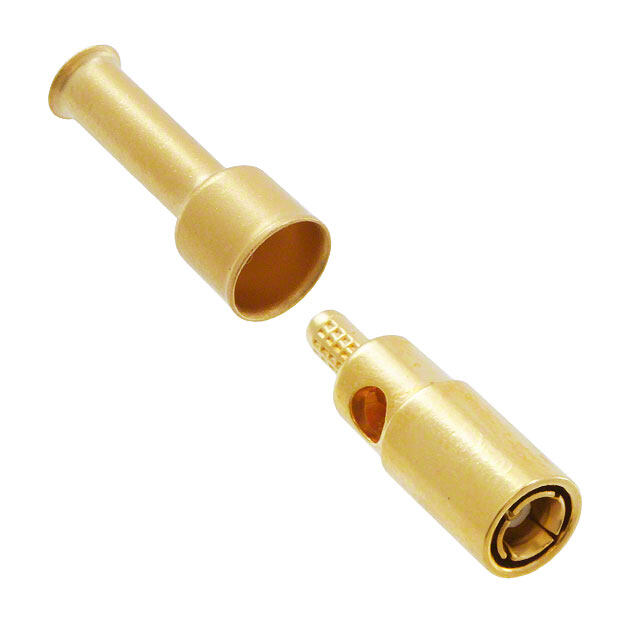
| 产品图片 |
|
| rohs | 符合RoHS无铅 / 符合限制有害物质指令(RoHS)规范要求 |
| 产品系列 | RF连接器/同轴连接器,Johnson / Cinch Connectivity Solutions 142-0761-821- |
| 数据手册 | |
| 产品型号 | 142-0761-821142-0761-821 |
| 中心触头材料 | 铜铍 |
| 中心触头镀层 | 金 |
| 主体材料 | Brass |
| 主体类型 | Right Angle |
| 主体表面处理 | Gold |
| 产品 | PCB Receptacles |
| 产品培训模块 | http://www.digikey.cn/PTM/IndividualPTM.page?site=cn&lang=zhs&ptm=24987 |
| 产品目录页面 | |
| 产品种类 | RF连接器/同轴连接器 |
| 介电材料 | 聚四氟乙烯(PTFE) |
| 侵入防护 | - |
| 保护端接 | |
| 其它名称 | 1420761821 |
| 包装 | 散装 |
| 商标 | Johnson / Cinch Connectivity Solutions |
| 型式 | Jack |
| 基体材料 | 黄铜 |
| 基体表面 | 金 |
| 外壳颜色 | 金 |
| 安装类型 | 板边缘,末端装入式 |
| 射频系列 | SMA |
| 工作温度 | -65°C ~ 165°C |
| 工作温度范围 | - 65 C to + 165 C |
| 工厂包装数量 | 5 |
| 方向 | Right Angle |
| 最大频率 | 26.5 GHz |
| 标准包装 | 25 |
| 特性 | - |
| 特色产品 | http://www.digikey.com/product-highlights/cn/zh/emerson-network-power-end-launch-connectors/1439 |
| 电缆组 | - |
| 相关产品 | /product-detail/zh/140-0000-973/J10081-ND/2059574 |
| 端接类型 | Solder |
| 系列 | SMA |
| 紧固类型 | 有螺纹 |
| 触头端接 | |
| 触点电镀 | Gold |
| 连接器样式 | SMA |
| 连接器类型 | 插孔, 母形插口 |
| 阻抗 | 50 欧姆50 Ohms |
| 频率-最大值 | 26.5GHz |
| 额定电压 | 170V |


- 商务部:美国ITC正式对集成电路等产品启动337调查
- 曝三星4nm工艺存在良率问题 高通将骁龙8 Gen1或转产台积电
- 太阳诱电将投资9.5亿元在常州建新厂生产MLCC 预计2023年完工
- 英特尔发布欧洲新工厂建设计划 深化IDM 2.0 战略
- 台积电先进制程称霸业界 有大客户加持明年业绩稳了
- 达到5530亿美元!SIA预计今年全球半导体销售额将创下新高
- 英特尔拟将自动驾驶子公司Mobileye上市 估值或超500亿美元
- 三星加码芯片和SET,合并消费电子和移动部门,撤换高东真等 CEO
- 三星电子宣布重大人事变动 还合并消费电子和移动部门
- 海关总署:前11个月进口集成电路产品价值2.52万亿元 增长14.8%


PDF Datasheet 数据手册内容提取
Cinch Connectivity Solutions High Frequency End Launch Connectors
HIGH FREQUENCY SMA END LAUNCH CONNECTORS Applications High Frequency SMA End Launch Connectors For Microwave PC Board Substrates The Johnson® Patent Pending High Frequency End Launch connectors are used to transition microwave energy from coaxial to planar transmission line structures. These patent pending connectors provide a unique solution for microwave engineers who fabricate circuit designs on very thin high frequency board substrates. The in-line connector design minimizes reflections as compared to a right-angle (perpendicular) pc mount transition. Applications for these connectors include: Cellular Linear Power Amplifiers Broadband MMIC Power Amplifiers Microwave Filters, Mixers and Combiners Wireless Infrastructure Antennas DBS Low-Noise Block Down Converters Remote Sensing and Metering Global Positioning Satellite Antennas Phased Array Antennas Radar Systems High Speed Routers and Switches Automated Test Equipment RF Identification Tags The Johnson® High Frequency End Launch connector is designed to attach directly to a high frequency coplanar waveguide (CPW) circuit board transmission line, although other lines such as microstrip can be used with good results. These connectors can be used on high frequency PC board substrate layers as thin as 8 mils, and operate at frequencies up to 26.5 GHz (see Return Loss chart). “PATENT PENDING” Typical Return Loss Measured on 50 ohm GCPW fabricated on Rogers® RO-4003™ substrate 142-0761-811 (8 mil substrate) 142-0761-871 (16 mil substrate) VSWR = 1.05+.02F(GHz) 2
HIGH FREQUENCY SMA END LAUNCH CONNECTORS Design Features This connector is an economical alternative to other high frequency designs in the industry. This patent pending design differentiates itself from other launch connectors: Design of the connector is self contained, no external mounting screws, adapter sections, spring clips, etc. are required for assembly to the circuit board. Center contact pin does not require special orientation to the surface of the circuit board. The center contact is mechanically captivated and optimized to maintain proper impedance while withstanding torque and axial force stress. Output coax of the connector at board launch is sized appropriately to match the thickness of the high frequency board substrate. The output coax section extends well within the connector while maintaining constant inner and outer coaxial diameters. Signal side grounding legs of the connector are spaced close enough to keep grounding paths short, but far enough apart to maintain constant impedance in the launch transition area. Signal side grounding legs and GCPW geometry control radiation, no additional shielding is required to prevent signal cross-talk effects in the transition area. The launch transition is effectively isolated from adjacent transmission lines in the signal plane. Connector is not locked into position when placed on the circuit board. Intentional floating design allows proper alignment in X, Y and Z, minimizing discontinuities due to manufacturing tolerances. The new distinctive through hole mounting technique allows the use of one connector with varying circuit board thicknesses. The connectors are also available in a traditional straddle mount end launch design, which was pioneered by Emerson Network Power Connectivity Solutions over 20 years ago. A small amount of PTFE insulation projects from the rear mating plane of the connector, acting as a seal when soldering the center conductor pin to the trace. The connector is held against the circuit board edge during the soldering process, compressing the PTFE insulation. This effectively creates a barrier between the inner and outer conductors, preventing the bridging of solder. Appropriate sized connectors do not require additional compensation to standard coplanar or microstrip matched impedance line geometries. Transition can be fine-tuned by pulling the trace back a slight amount from the board edge. cinchconnectivity.com 3
HIGH FREQUENCY SMA END LAUNCH CONNECTORS Specifications ELECTRICAL SPECIFICATIONS Mating Engagement for SMA Series Thickwall Impedance: 50 Ohms Plug Compatable with MIL-STD-348 Frequency Range: 0-26.5 GHz VSWR: 1.05+.02F(GHz) maximum at 0-18 GHz, <1.50 typical at 18-26.5 GHz Working Voltage: 170 Vrms maximum at sea level, 45 Vrms maximum at 70K feet Dielectric Withstanding Voltage: 500 Vrms minimum at sea level Corona Level: 125 Volts at 70K feet Insertion Loss: Dependant upon application Insulation Resistance: 1000 Megohms minimum Contact Resistance: (milliohms maximum) Initial After Environmental Center Contact . . . 3.0 4.0 Outer Conductor. . 2.0 Not Applicable RF Leakage: Not Applicable RF High Potential Withstanding Voltage: 335 Vrms minimum at 4 and 7 MHz MECHANICAL SPECIFICATIONS Engagement Design: MIL-STD-348, Series SMA Durability: 500 Cycles minimum Engagement/Disengagement Force: 2 inch-pounds maximum Mating Torque: 7 to 10 inch-pounds Contact Retention: 6 pounds minimum axial force, 4 in-oz minimum radial torque ENVIRONMENTAL SPECIFICATIONS (Meets or Exceeds the Applicable Paragraph of MIL-PRF-39012) Temperature Range: -65°C to +165°C Thermal Shock: MIL-STD-202, Method 107, Condition B-Except 115°C High Temp Corrosion: MIL-STD-202, Method 101, Condition B Shock: MIL-STD-202, Method 213, Condition I Vibration: MIL-STD-202, Method 204, Condition D Moisture Resistance: MIL-STD-202, Method 106 Assembly Tool for End Launch Jack Receptacles Hand tighten to 5 inch pounds maximum torque 140-0000-973 4
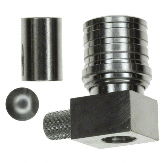
HIGH FREQUENCY SMA END LAUNCH CONNECTORS Part Data Jack Receptacle – PC Mount, Round Body Coupling proof torque 8 inch pounds maximum without support wrench Freq Range Gold Plated High Frequency Substrate Thickness “A” “B” “C” 142-0761-801 .008 (0.20) - .014 (0.36) .010 (0.25) .050 (1.27) .096 (2.44) 0-26.5 GHz 142-0761-821 .014 (0.36) - .020 (0.51) .015 (0.38) .067 (1.70) .113 (2.87) Jack Receptacle – PC Mount, Square Body Coupling proof torque 8 inch pounds maximum without support wrench Freq Range Gold Plated High Frequency Substrate Thickness “A” “B” “C” 142-0761-811 .008 (0.20) - .014 (0.36) .010 (0.25) .050 (1.27) .096 (2.44) 0-26.5 GHz 142-0761-831 .014 (0.36) - .020 (0.51) .015 (0.38) .067 (1.70) .113 (2.87) Jack Receptacle – PC Mount, Round Body with Thick Legs Freq Range Gold Plated High Frequency Substrate Thickness “A” “B” “C” 142-0761-881 .008 (0.20) - .014 (0.36) .010 (0.25) .050 (1.27) .096 (2.44) 0-26.5 GHz 142-0771-821 .014 (0.36) - .020 (0.51) .015 (0.38) .067 (1.70) .113 (2.87) cinchconnectivity.com 5
HIGH FREQUENCY SMA END LAUNCH CONNECTORS Part Data Jack Receptacle – Edge Mount for .062 Board, Round Body Coupling proof torque 8 inch pounds maximum without support wrench Freq Range Gold Plated High Frequency Substrate Thickness “A” “B” “C” 142-0761-841 .008 (0.20) - .014 (0.36) .010 (0.25) .050 (1.27) .032 (0.81) 0-26.5 GHz 142-0761-861 .014 (0.36) - .020 (0.51) .015 (0.38) .067 (1.70) .140 (1.02) Jack Receptacle – Edge Mount for .062 Board, Square Body Coupling proof torque 8 inch pounds maximum without support wrench Freq Range Gold Plated High Frequency Substrate Thickness “A” “B” “C” 142-0761-851 .008 (0.20) - .014 (0.36) .010 (0.25) .050 (1.27) .096 (2.44) 0-26.5 GHz 142-0761-871 .014 (0.36) - .020 (0.51) .015 (0.38) .067 (1.70) .113 (2.87) Jack Receptacle – Edge Mount for .062 Board, Round Body with Thick Legs Freq Range Gold Plated High Frequency Substrate Thickness “A” “B” 142-0761-891 .008 (0.20) - .014 (0.36) .010 (0.25) .050 (1.27) 0-26.5 GHz 142-0771-831 .014 (0.36) - .020 (0.51) .015 (0.38) .067 (1.70) 6
HIGH FREQUENCY SMA END LAUNCH CONNECTORS Mounting Instructions PC Mounting Instructions High frequency end launch performance is dependent upon proper mounting. The following factors must be controlled for optimum performance: a. The connector should fit tightly against the circuit board edge, avoid gaps. b. The center contact pin must lie parallel and flat against the circuit board, avoid gaps. c. The contact pin should be centered on the circuit board signal trace. d. Use a minimal amount of solder between the contact pin and signal trace. Do not allow excess solder to build up or flow down the trace. e. Clean all excess flux and other residue from the launch area, especially between the Figure 1 trace and ground The basic steps required to mount the end launch connector to the circuit board are as follows: 1. Fixture 140-0000-973 should be used as an aid during manual soldering. The fixture protects the connector from damage during clamping and also maintains the proper location of the connector’s insulator and contact. To use the fixture, thread the coupling nut on the mating end of the connector and hand tighten. This mounting Figure 2 assembly can now be held in a vice or similar clamping device, as shown in Figure 1. 2. Position connector on the circuit board, making sure the contact pin is aligned with the center of the signal trace as shown in Figure 2. Make sure that the connector legs and contact pin are held flush against the top of the circuit board, keeping the axis of the connector parallel to the plane of the circuit board, as shown in Figure 3. Figure 3 3. A small amount of Teflon® insulation projects from rear mating plane of the connector, which acts as a seal when soldering the center conductor pin to the trace. Clamp the connector ightly against the edge of the board. This action compresses the insulator seal against the board edge. This effectively creates a barrier between the inner and outer conductors preventing the bridging of solder. 4. While ensuring the connector is held in the correct position, solder the ground legs and/or ground posts to the top and bottom of the board prior to bonding the center pin to the trace. Figure 4 5. Once the connector body is properly grounded to the board, the center contact pin can be bonded to the trace by using a minimal amount of solder as shown in Figure 4.It is important that solder flows along the length of the exposed pin, creating a good electrical and mechanical connection. Remove any excess solder that is not required for a solid joint. 6. Clean all flux and other residues from the trace area between the signal side ground legs, as any flux present between the signal trace and ground will affect performance. The completed mounting assembly should look similar to the one shown in Figure 5. Figure 5 cinchconnectivity.com 7
HIGH FREQUENCY SMA END LAUNCH CONNECTORS Mounting Instructions Mounting Footprint Info 1. All of the drilled holes are plated through the entire circuit board stackup. 2. All hole patterns are symmetrical about center of the trace. 3. The recommended mounting footprints are shown for the top (signal) side of the board only. Use ground planes on additional layers where appropriate. 4. For optimum high frequency circuit board performance, use the following fabrication guidelines: a. Maintain a solid ground plane below the high frequency substrate layer. b. Control the pullback of the trace and grounds from the board edge. c. Continue the grounded coplanar waveguide line beyond the ground pad area. d. Place 16 mil diameter ground vias on both sides of the coplanar waveguide line, spaced at 50 mil intervals along the entire length of the line. e. Immersion gold plate (ENIG) all high frequency conductors per IPC-4552. f. Do not coat the coplanar waveguide signal trace or open ground gaps with soldermask. Reference dimensions for 50 ohm grounded coplanar waveguide using Rogers Corporation RO4003C™ high frequency substrate laminate* GCPW 50Ω Impedance Reference Dimensions * Mounting and Via Holes Substrate Conductor Trace Width Ground Gaps Part Number Fig “C” “D” Thickness Thickness “A” “B” 142-0761-801 .0080 (0.203) .0014 (0.036) .0155 (0.394) .0100 (0.254) 1 .066 (1.68) .096 (2.44) 142-0761-811 .0080 (0.203) .0014 (0.036) .0155 (0.394) .0100 (0.254) 1 .066 (1.68) .096 (2.44) 142-0761-821 .0160 (0.406) .0014 (0.036) .0285 (0.724) .0100 (0.254) 1 .084 (2.13) .113 (2.87) 142-0761-831 .0160 (0.406) .0014 (0.036) .0285 (0.724) .0100 (0.254) 1 .084 (2.13) .113 (2.87) 142-0761-841 .0080 (0.203) .0014 (0.036) .0155 (0.394) .0100 (0.254) 2 .066 (1.68) 142-0761-851 .0080 (0.203) .0014 (0.036) .0155 (0.394) .0100 (0.254) 2 .066 (1.68) 142-0761-861 .0160 (0.406) .0014 (0.036) .0285 (0.724) .0100 (0.254) 2 .084 (2.13) 142-0761-871 .0160 (0.406) .0014 (0.036) .0285 (0.724) .0100 (0.254) 2 .084 (2.13) 142-0761-881 .0080 (0.203) .0014 (0.036) .0155 (0.394) .0100 (0.254) 1 .066 (1.68) .096 (2.44) 142-0761-891 .0080 (0.203) .0014 (0.036) .0155 (0.394) .0100 (0.254) 2 .066 (1.68) 142-0761-821 .0160 (0.406) .0014 (0.036) .0285 (0.724) .0100 (0.254) 1 .084 (2.13) .113 (2.87)) 142-0761-831 .0160 (0.406) .0014 (0.036) .0285 (0.724) .0100 (0.254) 2 .084 (2.13) *These calculated dimensions assume a quasi-static mode of propagation, but dispersion does exist for coplanar waveguide. The characteristic impedance and effective dielectric constant may increase slightly for X-band and higher frequencies, unless very small ground to ground gap spacing is used. It is assumed the conductors have rectangular cross-sections. The Figure 1 etching process used in circuit board fabrication actually produces trapezoidal shapes. Therefore, the GCPW impedance may increase somewhere between that of a perfect rectangular conductor and a theoretical zero thickness conductor Figure 2 8
HIGH FREQUENCY SMA END LAUNCH CONNECTORS White Paper Low VSWR and Insertion Loss over a Wide Bandwidth An accurate characterization of packaged microwave circuits, such as broadband MMIC power amplifiers, requires coaxial to planar transitions with low return and insertion loss. In order to achieve low loss, the transition design between the launch connector and the printed circuit board requires the optimization of both mechanical and electrical features. The mechanical design must physically match the electromagnetic field distribution as close as possible in order to keep the discontinuity reactances small, as shown in Figure 1. The electrical design must match the impedances and other interface discontinuity reactances over the entire bandwidth. Minimizing the discontinuity reactances is desired rather than just compensating for them. Compensation can limit the usable frequency range of the connector, if the reactances are too large. The connector design incorporates an internal matched impedance transition from a large input coaxial connector interface, such as SMA, to a small coaxial output matched to the size of the PC board high frequency substrate. The internal transition between the input and output consists of graduated coaxial diametrical step sections, each optimized in size with inductive offsets to reduce the capacitive discontinuities created by the change in coaxial diameters. As shown in Figure 1, using multiple coaxial step sections to match the size of the circuit board reduces the overall effect of the discontinuities, thereby increasin the usable frequency range of the launch connector. The transition between the launch and the PC board is designed for attachment to grounded coplanar waveguide (GCPW) transmission lines. The signal output pin of the launcher is optimized in both length and diameter to match the corresponding GCPW line. The geometrical size of the signal side ground leg pairs is optimized in height, length and center to center spacing to match the output pin and GCPW line. The combination of optimal signal pin and ground leg design minimizes the attachment discontinuity reactance. Figure 1 - Simulated Electric Field Distributions within the Dielectric Regions at 18 GHz cinchconnectivity.com 9
HIGH FREQUENCY SMA END LAUNCH CONNECTORS White Paper Easily connected to GPCW transmission lines with reproducible results A coplanar waveguide transmission line is formed by a planar conductor separated by a pair of ground planes, all on the same plane, atop of a high frequency dielectric medium. A variant is formed when a ground plane is provided on the opposite side of the dielectric which is called grounded coplanar waveguide (GCPW). Although GCPW is the preferred transmission line structure on the circuit board for this connector, other lines such as microstrip can be used with good results. At microwave frequencies, the coplanar waveguide can be equal to or better than the microstrip when loss and dispersion are used as a basis for comparison. Minimum loss for a given coplanar waveguide occurs at about 60 Ohms whereas the minimum loss for microstrip occurs at about 25 Ohms. A full wave analysis Figure 1A which includes space wave and surface wave radiation shows that coplanar waveguide discontinuities radiate much less energy than microstrip discontinuities. The GCPW transmission line is fabricated on a high frequency circuit board substrate. Dielectric constant control, low dissipation factor and controlled thicknesses differentiate these high frequency circuit board materials from those typically used in the high volume printed circuit board world like FR4 and BT/epoxy. For higher frequencies, dielectric loss becomes an important contributor to the total loss. This is important because, as the frequency increases, the thickness of the material must Figure 1B decrease in order to avoid generating transverse modes on the Figure 1 - Simulated Electric Field Distributions transmission lines. within the Dielectric Regions at 18 GHz The high frequency material’s low loss performance extends the useful range of these materials well above 20 GHz. However, very thin dielectric layers as small as .008” are not mechanically stable enough to support the connector and associated circuitry. Therefore, hybrid circuit board constructions consisting of high frequency laminates and epoxy/glass substrates have become an increasingly utilized alternative to lower overall circuit board costs. The DC, control and digital signal paths are designed onto the lower cost epoxy/glass FR4 layer and the microwave signals are carried on the high frequency top layer as shown in Figures 1A and 1B. 10
HIGH FREQUENCY SMA END LAUNCH CONNECTORS White Paper As can be seen in the cut away portion of Figure 1, the connector’s center conductor pin is directly attached in-line with the GCPW signal trace. The body of the connector is always attached to the signal side ground. The design of the center conductor pin is a compromise between ease of assembly and minimal discontinuity reactance. The diameter of the pin is matched approximately to the thickness of the GCPW structure. Scaling down the pin diameter matches the electromagnetic field distributions with the GCPW line in order to keep the discontinuity reactance small. The output coax of the connector at the transition area is sized appropriately to match the thickness of the high frequency board substrate. The output coax section extends well within the connector by means of constant diameters, avoiding any abrupt diametrical changes at the circuit board edge which can create large discontinuities. Figure 1 - End Launch Connector Shown Attached to the GCPW Transmission Line cinchconnectivity.com 11
Cinch Connectivity Solutions is a global manufacturer of a broad line of connectivity products and services supporting wireline and wireless communications, data networking, test and measurement, military, medical, broadcast and industrial applications. Connectivity Solutions delivers custom-engineered products and solutions with best-in-class service and support and customer-focused offers such as quick-turn prototyping, samples and supply chain management. Precision Coaxial Connectors and Cable Assemblies Johnson - Subminiature, microminiature, miniature and standard connectors, and custom assemblies, including SMA, SMB, 40 GHz-capable SMK, MCX, MMCX, BNC Microwave Components CATV Components and N Connectors. Custom designs and Midwest Microwave - High Performance Viewsonics - Residential and multi-unit odifications of standard products. components including Attenuators, amplifiers, security terminators, and drop Terminations, Couplers, DC Blocks, Power splitters and passives. Headend signal Dividers, Phase Shifters, Adapters and management products and fiber optic High Performance Low Loss RF cable connectivity for headend and optical Assemblies. Able to offer QPL qualified node applications and return path test products. Standard components held in equipment. stock. Telecom/Broadband/OEM Cable Assemblies Custom solutions for the Telecom, Data Fiber Optic Cable Assemblies and Broadbandmarkets. Expert in 50 and Components position Telco cables, coax assemblies High performance multimode and single and analog filter products. Quick mode fiber patch cords, multi-fiber delivery capabilities. Custom solutions assemblies and attenuators. Solutions for for Multiconductor, Flat Ribbon, Wire the Storage Area Network and Enterprise Harness, Coaxial, D-sub, SCSI and computing markets and for ESCON™, discrete assemblies. Design support, optical FibreChannel, Infiniband and molding, polarizing, custom shielding and Parallel Optics applications. testing capabilities. Multi-purpose Connectivity and Structured Cabling Commercial-grade connectors, including F Connectors, BNC and TNC. Structured cabling components, including CAT 5E/6 assemblies, patch panels, wallplates and tools for data communications installations. USB and SCSI cables, D-sub connectors, adapters and hardware. 12
Cinch Connectivity Solutions High Frequency End Launch Connectors cinchconnectivity.com 13
Mouser Electronics Authorized Distributor Click to View Pricing, Inventory, Delivery & Lifecycle Information: C inch Connectivity Solutions: 142-0761-821