ICGOO在线商城 > 08055E104KAT2A
- 型号: 08055E104KAT2A
- 制造商: AVX
- 库位|库存: xxxx|xxxx
- 要求:
| 数量阶梯 | 香港交货 | 国内含税 |
| +xxxx | $xxxx | ¥xxxx |
查看当月历史价格
查看今年历史价格
08055E104KAT2A产品简介:
ICGOO电子元器件商城为您提供08055E104KAT2A由AVX设计生产,在icgoo商城现货销售,并且可以通过原厂、代理商等渠道进行代购。 提供08055E104KAT2A价格参考¥0.38-¥2.19以及AVX08055E104KAT2A封装/规格参数等产品信息。 你可以下载08055E104KAT2A参考资料、Datasheet数据手册功能说明书, 资料中有08055E104KAT2A详细功能的应用电路图电压和使用方法及教程。
| 参数 | 数值 |
| 产品目录 | |
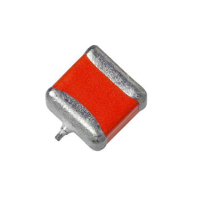
| 描述 | CAP CER 0.1UF 50V 10% Z5U 0805多层陶瓷电容器MLCC - SMD/SMT 50volts 0.1uF 10% Z5U |
| 产品分类 | |
| 品牌 | AVX |
| 产品手册 | |
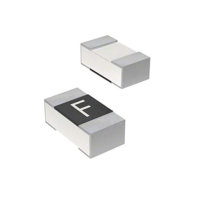
| 产品图片 |
|
| rohs | 符合RoHS无铅 / 符合限制有害物质指令(RoHS)规范要求 |
| 产品系列 | MLCC,多层陶瓷电容器MLCC - SMD/SMT,AVX 08055E104KAT2A- |
| 数据手册 | |
| 产品型号 | 08055E104KAT2A |
| 产品 | General Type MLCCs |
| 产品种类 | 多层陶瓷电容器MLCC - SMD/SMT |
| 加载寿命 | 1000 h |
| 包装 | 带卷 (TR) |
| 厚度(最大值) | 0.037"(0.94mm) |
| 商标 | AVX |
| 外壳代码-in | 0805 |
| 外壳代码-mm | 2012 |
| 大小/尺寸 | 0.079" 长 x 0.049" 宽(2.00mm x 1.25mm) |
| 安装类型 | 表面贴装,MLCC |
| 容差 | 10 % |
| 封装 | Reel |
| 封装/外壳 | 0805(2012 公制) |
| 封装/箱体 | 0805 (2012 metric) |
| 工作温度 | 10°C ~ 85°C |
| 工作温度范围 | - 55 C to + 125 C |
| 工厂包装数量 | 4000 |
| 应用 | 通用 |
| 引线形式 | - |
| 引线间距 | - |
| 最大工作温度 | + 125 C |
| 最小工作温度 | - 55 C |
| 标准包装 | 4,000 |
| 温度系数 | Z5U |
| 温度系数/代码 | +/- 15 % |
| 特性 | - |
| 电介质 | X7R |
| 电压-额定 | 50V |
| 电压额定值 | 50 V |
| 电压额定值DC | 50 V |
| 电容 | 0.1 uF |
| 端接类型 | SMD/SMT |
| 等级 | - |
| 类型 | Z5U Dielectric |
| 高度-安装(最大值) | - |




- 商务部:美国ITC正式对集成电路等产品启动337调查
- 曝三星4nm工艺存在良率问题 高通将骁龙8 Gen1或转产台积电
- 太阳诱电将投资9.5亿元在常州建新厂生产MLCC 预计2023年完工
- 英特尔发布欧洲新工厂建设计划 深化IDM 2.0 战略
- 台积电先进制程称霸业界 有大客户加持明年业绩稳了
- 达到5530亿美元!SIA预计今年全球半导体销售额将创下新高
- 英特尔拟将自动驾驶子公司Mobileye上市 估值或超500亿美元
- 三星加码芯片和SET,合并消费电子和移动部门,撤换高东真等 CEO
- 三星电子宣布重大人事变动 还合并消费电子和移动部门
- 海关总署:前11个月进口集成电路产品价值2.52万亿元 增长14.8%



PDF Datasheet 数据手册内容提取
Z5U Dielectric General Specifications Z5U formulations are “general-purpose” ceramics which are meant primarily for use in limited temperature applications where small size and cost are important. Z5U show wide variations in capacitance under influence of environmental and electrical operating conditions. Despite their capacitance instability, Z5U formulations are very popular because of their small size, low ESL, low ESR and excellent frequency response. These features are particularly important for decoupling application where only a minimum capacitance value is required. PART NUMBER (see page 3 for complete part number explanation) 0805 5 E 104 Z A T 2 A Size Voltage Dielectric Capacitance Capacitance Failure Terminations Packaging Special (L" x W") 25V = 3 Z5U = E Code Tolerance Rate T = Plated Ni 2 = 7" Reel Code 50V = 5 Preferred A = Not and Solder 4 = 13" Reel A = Std. Z = +80% Applicable Product –20% M = ±20% PERFORMANCE CHARACTERISTICS Capacitance Range 0.01 µF to 1.0 µF Capacitance Tolerances Preferred +80 –20% others available: ±20%, +100 –0% Operating Temperature Range +10°C to +85°C Temperature Characteristic +22% to –56% max. Voltage Ratings 25 and 50VDC (+85°C) Dissipation Factor 4% max. Insulation Resistance (+25°C, RVDC) 10,000 megohms min. or 1000 MΩ- µF min., whichever is less Dielectric Strength 250% of rated voltage for 5 seconds at 50 mamp max. current Test Voltage 0.5 ±0.2 Vrms Test Frequency 1 KHz 12
Z5U Dielectric Typical Characteristic Curves** Temperature Coefficient Variation of Impedance with Cap Value +30 Impedance vs. Frequency +20 1206 -Z5U e +10 nc 0 100.00 acita --1200 p -30 Ca -40 10.00 D% --5600 Ve, 10,000 pF c an 1.00 d +10 +25 +30+35 +40 +45 +50 +55 +65 +85 pe 100,000 pF Temperature °C m I 0.10 0.01 1 10 100 1,000 Frequency, MHz Variation of Impedance with Chip Size D Capacitance vs. Frequency Impedance vs. Frequency .33 mF - Z5U 1000 ce 0 n Z5U 1206 acita -10 100 ZZ55UU 11281102 Cap -20 ms) D oh 10 % -30 Z| ( | -40 1 1KHz 10 KHz 100 KHz 1 MHz 10 MHz Frequency 0.1 0.001 0.01 0.1 1 10 100 1,000 Frequency, MHz Variation of Impedance with Ceramic Formulation s) nsuation Resistance vs Temperature Impedance vs. Frequency ad100,000 .1mF X7R vs. Z5U ar 0805 F m- 10000 e (Oh 10,000 1000 XZ75RU 00880055 anc 1,000 s) 100 st m on Resi 100 |Z| (oh 101 ulati 0 +20 +30 +40 +50 +60 +70 +80 0.1 s In Temperature °C 0.01 0.001 0.01 0.1 1 10 100 1,000 Frequency, MHz SUMMARY OF CAPACITANCE RANGES VS. CHIP SIZE Style 25V 50V 0603* .01µF - .047µF .01µF - .027µF 0805* .01µF - .12µF .01µF - 0.1µF 1206* .01µF - .33µF .01µF - .33µF 1210* .01µF - .56µF .01µF - .47µF 1808 .01µF - .56µF .01µF - .47µF 1812* .01µF - 1.0µF .01µF - 1.0µF 1825* .01µF - 1.0µF .01µF - 1.0µF 2225 .01µF - 1.0µF .01µF - 1.0µF * Standard Sizes **For additional information on performance changes with operating conditions consult AVX’s software SpiCap. 13
Z5U Dielectric Capacitance Range PREFERRED SIZES ARE SHADED SIZE 0603* 0805 1206 1210 Standard Reel Packaging All Paper Paper/Embossed Paper/Embossed Paper/Embossed MM 1.60 ±.15 2.01 ±.20 3.20 ±.20 3.20 ±.20 (L) Length (in.) (.063 ±.006) (.079 ±.008) (.126 ±.008) (.126 ±.008) MM .81 ±.15 1.25 ±.20 1.60 ±.20 2.50 ±.20 (W) Width (in.) (.032 ±.006) (.049 ±.008) (.063 ±.008) (.098 ±.008) MM .90 1.30 1.50 1.70 (T) Max. Thickness (in.) (.035) (.051) (.059) (.067) MM .35 ±.15 .50 ±.25 .50 ±.25 .50 ±.25 (t) Terminal (in.) (.014 ±.006) (.020 ±.010) (.020 ±.010) (.020 ±.010) WVDC 25 50 25 50 25 50 25 50 Cap .010 . . W (µF) .012 L . . . .015 T .018 . .022 .027 .t. .033 .039 .047 .056 .068 .082 .10 .12 .15 .18 .22 .27 .33 .39 .47 .56 .68 .82 1.0 1.5 *Reflow soldering only. = Paper Tape = Embossed Tape NOTES:For low profile chips, see page 19. 14
Z5U Dielectric Capacitance Range PREFERRED SIZES ARE SHADED SIZE 1808* 1812* 1825* 2225* Standard Reel Packaging All Embossed All Embossed All Embossed All Embossed MM 04.57 ±.25 4.50 ±.30 4.50 ±.30 5.72 ±.25 (L) Length (in.) (.180 ±.010) (.177 ±.012) (.177 ±.012) (.225 ±.010) MM 2.03 ±.25 3.20 ±.20 6.40 ±.40 6.35 ±.25 (W) Width (in.) (.080 ±.010) (.126 ±.008) (.252 ±.016) (.250 ±.010) MM 1.52 1.70 1.70 1.70 (T) Max. Thickness (in.) (.060) (.067) (.067) (.067) MM .64 ±.39 .61 ±.36 .61 ±.36 .64 ±.39 (t) Terminal (in.) (.025 ±.015) (.024 ±.014) (.024 ±.014) (.025 ±.015) WVDC 25 50 25 50 25 50 25 50 Cap .010 (µF) .012 .015 . . W .018 L . .022 . .T . .027 .033 .039 .t. .047 .056 .068 .082 .10 .12 .15 .18 .22 .27 .33 .39 .47 .56 .68 .82 1.0 1.5 *Reflow soldering only. = Paper Tape = Embossed Tape NOTES: For low profile chips, see page 19. 15
Basic Capacitor Formulas I. Capacitance (farads) XI. Equivalent Series Resistance (ohms) English: C = .224 K A E.S.R. = (D.F.) (Xc) = (D.F.) / (2 πfC) T D XII. Power Loss (watts) Metric: C = .0884 K A Power Loss = (2 πfCV2) (D.F.) T D XIII. KVA (Kilowatts) II. Energy stored in capacitors (Joules, watt - sec) KVA = 2 πfCV2x 10-3 E = 1⁄2 CV2 XIV. Temperature Characteristic (ppm/°C) III. Linear charge of a capacitor (Amperes) dV T.C. = Ct – C25 x 106 I = C C (T – 25) dt 25 t IV. Total Impedance of a capacitor (ohms) XV. Cap Drift (%) ˛ C – C Z = R2 + (XC- XL)2 C.D. = 1 2 x 100 S C 1 V. Capacitive Reactance (ohms) XVI. Reliability of Ceramic Capacitors 1 xc= 2 πfC L0= (Vt ) X (Tt ) Y L V T t o o VI. Inductive Reactance (ohms) XVII. Capacitors in Series (current the same) x = 2 πfL L Any Number: 1 = 1 + 1 --- 1 VII. Phase Angles: CT C1 C2 CN Ideal Capacitors: Current leads voltage 90° C C Ideal Inductors: Current lags voltage 90° Two: CT= C 1+ C2 1 2 Ideal Resistors: Current in phase with voltage XVIII. Capacitors in Parallel (voltage the same) VIII. Dissipation Factor (%) D.F.= tan d(loss angle) = E.S.R. = (2 πfC) (E.S.R.) CT= C1+ C2---+ CN Xc XIX. Aging Rate IX. Power Factor (%) A.R. = %DC/decade of time P.F. = Sine d(loss angle) = Cos f(phase angle) XX. Decibels P.F. = (when less than 10%) = DF V db = 20 log 1 X. Quality Factor (dimensionless) V 2 Q = Cotan d(loss angle) = 1 D.F. METRIC PREFIXES SYMBOLS Pico X 10-12 K = Dielectric Constant f = frequency L = Test life t Nano X 10-9 Micro X 10-6 A = Area L = Inductance Vt = Test voltage Milli X 10-3 T = Dielectric thickness d = Loss angle V = Operating voltage Deci X 10-1 D o Deca X 10+1 V = Voltage f = Phase angle Tt = Test temperature Kilo X 10+3 Mega X 10+6 t = time X & Y = exponent effect of voltage and temp. T = Operating temperature o Giga X 10+9 Tera X 10+12 Rs = Series Resistance Lo = Operating life 2
How to Order Part Number Explanation EXAMPLE: 08055A101JAT2A 0805 5 A 101 J A T 2 A Size Dielectric Capacitance Terminations Special** (L" x W") C0G (NP0) = A Tolerance Code 0402 X7R = C C = ±.25 pF* Standard: A = Standard 0504 X5R = D D = ±.50 pF* T = Ni and Tin Product 0603 Z5U = E F = ±1% (‡ 25 pF) Plated Non-Standard 0805 Y5V = G G = ±2% (‡ 13 pF) P = Embossed 1005 J = ±5% Others: unmarked 0907 K = ±10% 7 = Plated Ni M = Embossed 1206 M = ±20% Gold Plated marked 1210 Z = +80%, -20% 1 = Pd/Ag E = Standard 1505 P = +100%, -0% packaging 1805 marked 1808 Low Profile 1812 Chips Only 1825 Max. Thickness 2225 Voltage Capacitance Failure T = .66mm (.026") 3640 10V = Z Code Rate S = .56mm (.022") 16V = Y (2 significant A = Not R = .46mm (.018") 25V = 3 digits + no. of Applicable 50V = 5 zeros) 100V = 1 Examples: Packaging** 200V = 2 10 pF =100 250V = V 100 pF =101 Recommended: 500V = 7 1,000 pF =102 2 =7" Reel 600V =C 22,000 pF =223 4 =13" Reel 1000V =A 220,000 pF =224 1500V =S 1 µF =105 2000V =G Others: For values below 10 pF, 2500V =W 7 = Bulk Cassette use “R” in place of 3000V =H 9 = Bulk decimal point, e.g., 9.1 4000V = J pfd = 9R1. 5000V =K *C&D tolerances for #10 pF values. ** Standard Tape and Reel material depends upon chip size and thickness. See individual part tables for tape material type for each capacitance value. Note: Unmarked product is standard. Marked product is available on special request, please contact AVX. Standard packaging is shown in the individual tables. Non-standard packaging is available on special request, please contact AVX. 3
General Specifications Environmental THERMAL SHOCK MOISTURE RESISTANCE Specification Specification Appearance Appearance No visual defects No visual defects Capacitance Variation Capacitance Variation C0G (NP0): ±2.5% or ±.25pF, whichever is greater C0G (NP0): ±5% or ±.5pF, whichever is greater X7R: ≤±7.5% X7R: ≤±10% Z5U: ≤±20% Z5U: ≤±30% Y5V: ≤±20% Y5V: ≤±30% Q, Tan Delta Q, Tan Delta To meet initial requirement C0G (NP0):‡ 30pF........................Q ‡ 350 ‡ 10pF, < 30pF...........Q ‡ 275+5C/2 Insulation Resistance < 10pF........................Q ‡ 200+10C C0G (NP0), X7R: To meet initial requirement Z5U, Y5V: ‡ Initial Value x 0.1 X7R:Initial requirement + .5% Z5U:Initial requirement + 1% Dielectric Strength Y5V:Initial requirement + 2% No problem observed Measuring Conditions Insulation Resistance ‡ Initial Value x 0.3 Step Temperature °C Time (minutes) C0G (NP0), X7R: -55°±2° Measuring Conditions 1 Z5U: +10°±2° 30 ±3 Step Temp. °C Humidity % Time (hrs) Y5V: -30°±2° 1 +25->+65 90-98 2.5 2 Room Temperature # 3 2 +65 90-98 3.0 3 C0G (NP0), X7R: +125°±2° 30 ±3 3 +65->+25 80-98 2.5 Z5U, Y5V: +85°±2° 4 +25->+65 90-98 2.5 4 Room Temperature # 3 5 +65 90-98 3.0 6 +65->+25 80-98 2.5 Repeat for 5 cycles and measure after 48 hours ±4 hours 7 +25 90-98 2.0 (24 hours for C0G (NP0)) at room temperature. 7a -10 uncontrolled – IMMERSION 7b +25 90-98 – Specification Repeat 20 cycles (1-7) and store for 48 hours (24 hours for C0G (NP0)) at room temperature before measuring. Appearance Steps 7a & 7b are done on any 5 out of first 9 cycles. No visual defects Capacitance Variation C0G (NP0): ±2.5% or ±.25pF, whichever is greater X7R: ≤±7.5% Z5U: ≤±20% Y5V: ≤±20% Q, Tan Delta To meet initial requirement Insulation Resistance C0G (NP0), X7R: To meet initial requirement Z5U, Y5V: ‡ Initial Value x 0.1 Dielectric Strength No problem observed Measuring Conditions Step Temperature °C Time (minutes) +65 +5/-0 1 15 ±2 Pure Water 0 ±3 2 15 ±2 NaCl solution Repeat cycle 2 times and wash with water and dry. Store at room temperature for 48 ± 4 hours (24 hours for C0G (NP0)) and measure. 22
General Specifications Environmental STEADY STATE HUMIDITY Insulation Resistance (No Load) C0G (NP0), X7R: To meet initial value x 0.3 Specification Z5U, Y5V: ‡ Initial Value x 0.1 Appearance Charge devices with rated voltage in test chamber set No visual defects at 85 ± 5% relative humidity and 85°C for 1000 (+48,-0) hours. Remove from test chamber and Capacitance Variation stabilize at room temperature and humidity for 48 ± 4 C0G (NP0): ±5% or ±.5pF, whichever is greater X7R: ≤±10% hours (24 ±2 hours for C0G (NP0)) before measuring. Z5U: ≤±30% Charge and discharge currents must be less than Y5V: ≤±30% 50ma. Q, Tan Delta C0G (NP0): ‡ 30pF......................Q ‡ 350 ‡ 10pF,< 30pF.........Q ‡ 275+5C/2 LOAD LIFE < 10pF ....................Q ‡ 200+10C X7R: Initial requirement + .5% Specification Z5U:Initial requirement + 1% Appearance Y5V:Initial requirement + 2% No visual defects Insulation Resistance Capacitance Variation ‡ Initial Value x 0.3 C0G (NP0): ±3% or ±.3pF, whichever is greater Measuring Conditions X7R: ≤±10% Z5U: ≤±30% Store at 85 ± 5% relative humidity and 85°C for 1000 Y5V: ≤±30% hours, without voltage. Remove from test chamber and stabilize at room temperature and humidity for Q, Tan Delta 48 ± 4 hours (24 ±2 hours for C0G (NP0)) before C0G (NP0): ‡ 30pF......................Q ‡ 350 measuring. ‡ 10pF,< 30pF.........Q ‡ 275+5C/2 < 10pF ....................Q ‡ 200+10C Charge and discharge currents must be less than X7R: Initial requirement + .5% 50ma. Z5U:Initial requirement + 1% Y5V:Initial requirement + 2% LOAD HUMIDITY Insulation Resistance C0G (NP0), X7R: To meet initial value x 0.3 Specification Z5U, Y5V: ‡ Initial Value x 0.1 Appearance Charge devices with twice rated voltage in test No visual defects chamber set at +125°C ±2°C for C0G (NP0) and X7R, +85°± 2°C for Z5U, and Y5V for 1000 (+48,-0) hours. Capacitance Variation Remove from test chamber and stabilize at room C0G (NP0): ±5% or ±.5pF, whichever is greater temperature for 48 ± 4 hours (24 ±2 hours for C0G X7R: ≤±10% (NP0)) before measuring. Z5U: ≤±30% Y5V: ≤±30% Charge and discharge currents must be less than 50ma. Q, Tan Delta C0G (NP0): ‡ 30pF.....................Q ‡ 350 ‡ 10pF,< 30pF.........Q ‡ 275+5C/2 < 10pF ....................Q ‡ 200+10C X7R: Initial requirement + .5% Z5U:Initial requirement + 1% Y5V:Initial requirement + 2% 23
General Specifications Mechanical END TERMINATION ADHERENCE BEND STRENGTH Specification Speed = 1mm/sec No evidence of peeling of end terminal 2mm Measuring Conditions Deflection R340mm After soldering devices to circuit board apply 5N (0.51kg f) for 10 ±1 seconds, please refer to Figure 1. 45mm 45mm Supports 5N FORCE Figure 2. Bend Strength Specification DEVICE UNDER TEST Appearance: Figure 1. No visual defects TEST BOARD Terminal Adhesion Capacitance Variation C0G (NP0): ±5% or ±.5pF, whichever is larger RESISTANCE TO VIBRATION X7R: ≤±12% Z5U: ≤±30% Specification Y5V: ≤±30% Appearance: Insulation Resistance No visual defects C0G (NP0): ‡ Initial Value x 0.3 Capacitance X7R: ‡ Initial Value x 0.3 Within specified tolerance Z5U: ‡ Initial Value x 0.1 Q, Tan Delta Y5V: ‡ Initial Value x 0.1 To meet initial requirement Measuring Conditions Insulation Resistance Please refer to Figure 2 C0G (NP0), X7R $Initial Value x 0.3 Deflection: Z5U, Y5V $Initial Value x 0.1 2mm Measuring Conditions Test Time: Vibration Frequency 30 seconds 10-2000 Hz RESISTANCE TO SOLDER HEAT Maximum Acceleration 20G Specification Swing Width Appearance: 1.5mm No serious defects, <25% leaching of either end Test Time terminal X, Y, Z axis for 2 hours each, total 6 hours of test Capacitance Variation C0G (NP0): ±2.5% or ±2.5pF, whichever is greater SOLDERABILITY X7R: ≤±7.5% Z5U: ≤±20% Specification Y5V: ≤±20% $95% of each termination end should be covered with Q, Tan Delta fresh solder To meet initial requirement Measuring Conditions Insulation Resistance Dip device in eutectic solder at 230 ±5°C for To meet initial requirement 2 ±.5 seconds Dielectric Strength No problem observed Measuring Conditions Dip device in eutectic solder at 260°C, for 1 minute. Store at room temperature for 48 hours (24 hours for C0G (NP0)) before measuring electrical parameters. Part sizes larger than 3.20mm x 2.49mm are reheated at 150°C for 30 ±5 seconds before performing test. 24
European Detail Specifications CECC 32 101-801/Chips Standard European Ceramic Chip Capacitors PART NUMBER (example) 0805 5 C 103 M T T 2 A Size Voltage Dielectric Capacitance Capacitance Specification Terminations Marking Special (L" x W") 50V = 5 1B CG = A Code Tolerance CECC32101-801 T = Plated Ni Packaging Code 100V = 1 2R1 = C See Dielectrics and Sn 2 = 7" Reel A = Std. 200V = 2 2F4 = G C0G, X7R, Y5V 4 = 13" Reel Product RANGE OF APPROVED COMPONENTS Case Dielectric Voltage and Capacitance Range Size Type 50V 100V 200V 1BCG 0603 1B CG 0.47pF - 150pF 0.47pF - 120pF 0.47pF - 100pF 0805 1B CG 0.47pF - 560pF 0.47pF - 560pF 0.47pF - 330pF 1206 1B CG 0.47pF - 3.3nF 0.47pF - 3.3nF 0.47pF - 1.5nF 1210 1B CG 0.47pF - 4.7nF 0.47pF - 4.7nF 0.47pF - 2.7nF 1808 1B CG 0.47pF - 6.8nF 0.47pF - 6.8nF 0.47pF - 4.7nF 1812 1B CG 0.47pF - 15nF 0.47pF - 15nF 0.47pF - 10nF 2220 1B CG 0.47pF - 39nF 0.47pF - 39nF 0.47pF - 15nF 2R1 0603 2R1 10pF - 6.8nF 10pF - 6.8nF 10pF - 1.2nF 0805 2R1 10pF - 33nF 10pF - 18nF 10pF - 3.3nF 1206 2R1 10pF - 100nF 10pF - 68nF 10pF - 18nF 1210 2R1 10pF - 150nF 10pF - 100nF 10pF - 27nF 1808 2R1 10pF - 270nF 10pF - 180nF 10pF - 47nF 1812 2R1 10pF - 470nF 10pF - 330nF 10pF - 100nF 2220 2R1 10pF - 1.2µF 10pF - 680nF 10pF - 220nF 2F4 0805 2F4 10pF - 100nF 1206 2F4 10pF - 330nF 1210 2F4 10pF - 470nF 1808 2F4 10pF - 560nF 1812 2F4 10pF - 1.8µF 2220 2F4 10pF - 2.2µF 31
Packaging of Chip Components Automatic Insertion Packaging TAPE & REEL QUANTITIES All tape and reel specifications are in compliance with RS481. 8mm 12mm Paper or Embossed Carrier 0805, 1005, 1206, 1210 Embossed Only 0504, 0907 1505, 1805, 1812, 1825 1808 2220, 2225 Paper Only 0402, 0603 Qty. per Reel/7" Reel 2,000 or 4,000(1) 3,000 1,000 Qty. per Reel/13" Reel 10,000 10,000 4,000 (1)Dependent on chip thickness. Low profile chips shown on page 27 are 5,000 per reel for 7" reel. 0402 size chips are 10,000 per 7" reels and are not available on 13" reels. For 3640 size chip contact factory for quantity per reel. REEL DIMENSIONS Tape A B* D* N W C W 2 W Size(1) Max. Min. Min. Min. 1 Max. 3 7.9 Min. 8.4+1.0 14.4 (.311) 8mm –0.0 (.331+.060) (.567) 10.9 Max. –0.0 (.429) 330 1.5 13.0±0.20 20.2 50 (12.992) (.059) (.512±.008) (.795) (1.969) 11.9 Min. 12.4+2.0 18.4 (.469) 12mm –0.0 (.488+.076) (.724) 15.4 Max. –0.0 (.607) Metric dimensions will govern. English measurements rounded and for reference only. (1) For tape sizes 16mm and 24mm (used with chip size 3640) consult EIA RS-481 latest revision. 32
Embossed Carrier Configuration 8 & 12mm Tape Only 8 & 12mm Embossed Tape Metric Dimensions Will Govern CONSTANT DIMENSIONS Tape Size D E P P TMax. T G G 0 0 2 1 1 2 8mm 8.4+0.10 1.75 ±0.10 4.0 ±0.10 2.0 ±0.05 0.600 0.10 0.75 0.75 -0.0 and (.059+.004) (.069 ±.004) (.157 ±.004) (.079 ±.002) (.024) (.004) (.030) (.030) -0.0 12mm Max. Min. Min. See Note 3 SeeNote 4 VARIABLE DIMENSIONS Tape Size B D F P R T W A B K 1 1 1 2 0 0 0 Max. Min. Min. See Note 6 See Note 5 See Note 2 4.55 1.0 3.5 ±0.05 4.0 ±0.10 25 2.5 Max 8.0+0.3 8mm (.179) (.039) (.138 ±.002) (.157 ±.004) (.984) (.098) (.315-+0..0112 ) See Note 1 -.004 8.2 1.5 5.5 ±0.05 4.0 ±0.10 30 6.5 Max. 12.0 ±.30 12mm (.323) (.059) (.217 ±.002) (.157 ±.004) (1.181) (.256) (.472 ±.012) See Note 1 8mm 4.55 1.0 3.5 ±0.05 2.0 ±0.10 25 2.5 Max. 8.0+0.3 1/2 Pitch (.179) (.039) (.138 ±.002) 0.79 ±.004 (.984) (.098) (.315-+0..0112 ) See Note 1 -.004 12mm Double 8.2 1.5 5.5 ±0.05 8.0 ±0.10 30 6.5 Max. 12.0 ±.30 See Note 1 (.323) (.059) (.217 ±.002) (.315 ±.004) (1.181) (.256) (.472 ±.012) Pitch NOTES: 1. A, B, and K are determined by the max. dimensions to the ends of the terminals extending from the component body and/or the body dimensions of the component. The 0 0 0 clearance between the end of the terminals or body of the component to the sides and depth of the cavity (A, B, and K) must be within 0.05 mm (.002) min. and 0.50 mm 0 0 0 (.020) max. The clearance allowed must also prevent rotation of the component within the cavity of not more than 20 degrees (see sketches C &D). 2. Tape with components shall pass around radius “R” without damage. The minimum trailer length (Note 2 Fig. 3) may require additional length to provide R min. for 12 mm embossed tape for reels with hub diameters approaching N min. (Table 4). 3. G dimension is the flat area from the edge of the sprocket hole to either the outward deformation of the carrier tape between the embossed cavities or to the edge of the 1 cavity whichever is less. 4. G dimension is the flat area from the edge of the carrier tape opposite the sprocket holes to either the outward deformation of the carrier tape between the embossed cavity 2 or to the edge of the cavity whichever is less. 5. The embossment hole location shall be measured from the sprocket hole controlling the location of the embossment. Dimensions of embossment location and hole location shall be applied independent of each other. 6. B dimension is a reference dimension for tape feeder clearance only. 1 33
Paper Carrier Configuration 8 & 12mm Tape Only 8 & 12mm Paper Tape Metric Dimensions Will Govern CONSTANT DIMENSIONS Tape Size D E P P T G G R MIN. 0 0 2 1 1 2 8mm 1.5 +0.1 1.75 ±0.10 4.0 ±0.10 2.0 ±0.05 0.10 0.75 0.75 25 (.984) -0.0 and (.059+.004) (.069 ±.004) (.157 ±.004) (.079 ±.002) (.004) (.030) (.030) See Note 2 -.000 12mm Max. Min. Min. VARIABLE DIMENSIONS Tape Size P F W A B T 1 0 0 8mm 4.0 ±0.10 3.5 ±0.05 8.0+0.3 See Note 1 See Note 3 -0.1 (.157 ±.004) (.138 ±.002) (.315+.012 ) -.004 4.0 ±.010 5.5 ±0.05 12.0 ±0.3 12mm (.157 ±.004) (.217 ±.002) (.472 ±.012) 8mm 2.0 ±0.10 3.5 ±0.05 8.0+0.3 -0.1 1/2 Pitch (.079 ±.004) (.138 ±.002) (.315+.012 ) -.004 12mm 8.0 ±0.10 5.5 ±0.05 12.0 ±0.3 Double (.315 ±.004) (.217 ±.002) (.472 ±.012) Pitch NOTES: 1. A, B, and T are determined by the max. dimensions to the ends of the terminals extending from the component body and/or the body dimensions of the component. The 0 0 clearance between the ends of the terminals or body of the component to the sides and depth of the cavity (A, B, and T) must be within 0.05 mm (.002) min. and 0.50 mm 0 0 (.020) max. The clearance allowed must also prevent rotation of the component within the cavity of not more than 20 degrees (see sketches A &B). 2. Tape with components shall pass around radius “R” without damage. 3. 1.1 mm (.043) Base Tape and 1.6 mm (.063) Max. for Non-Paper Base Compositions. Bar Code Labeling Standard AVX bar code labeling is available and follows latest version of EIA-556-A. 34
Bulk Case Packaging BENEFITS BULK FEEDER • Easier handling • Smaller packaging volume (1/20 of T/R packaging) • Easier inventory control Case • Flexibility • Recyclable Cassette Gate Shooter CASE DIMENSIONS Shutter Slider 12mm 36mm Mounter Expanded Drawing Head 110mm Chips Attachment Base CASE QUANTITIES Part Size 0402 0603 0805 Qty. 10,000 (T=0.6mm) 80,000 15,000 (pcs / cassette) 5,000 (T¯‡ 0.6mm) 35
General Description Basic Construction – A multilayer ceramic (MLC) capaci- structure requires a considerable amount of sophistication, tor is a monolithic block of ceramic containing two sets of both in material and manufacture, to produce it in the quality offset, interleaved planar electrodes that extend to two and quantities needed in today’s electronic equipment. opposite surfaces of the ceramic dielectric. This simple Electrode Ceramic Layer End Terminations Terminated Edge Terminated Edge Margin Electrodes Formulations – Multilayer ceramic capacitors are available Class 2 – EIA Class 2 capacitors typically are based on the in both Class 1 and Class 2 formulations. Temperature chemistry of barium titanate and provide a wide range of compensating formulation are Class 1 and temperature capacitance values and temperature stability. The most stable and general application formulations are classified commonly used Class 2 dielectrics are X7R and Y5V. The as Class 2. X7R provides intermediate capacitance values which vary only ±15% over the temperature range of -55°C to 125°C. It finds applications where stability over a wide temperature Class 1 – Class 1 capacitors or temperature compensating range is required. capacitors are usually made from mixtures of titanates where barium titanate is normally not a major part of the The Y5V provides the highest capacitance values and is mix. They have predictable temperature coefficients and used in applications where limited temperature changes are in general, do not have an aging characteristic. Thus they expected. The capacitance value for Y5V can vary from are the most stable capacitor available. The most popular 22% to -82% over the -30°C to 85°C temperature range. Class 1 multilayer ceramic capacitors are C0G (NP0) The Z5U dielectric is between X7R and Y5V in both stability temperature compensating capacitors (negative-positive and capacitance range. 0 ppm/°C). All Class 2 capacitors vary in capacitance value under the influence of temperature, operating voltage (both AC and DC), and frequency. For additional information on perfor- mance changes with operating conditions, consult AVX’s software, SpiCap. 36
General Description Effects of Voltage – Variations in voltage have little effect Cap. Change vs. D.C. Volts on Class 1 dielectric but does affect the capacitance and AVX X7R T.C. dissipation factor of Class 2 dielectrics. The application of DC voltage reduces both the capacitance and dissipation nt 2.5 e factor while the application of an AC voltage within a c er 0 reasonable range tends to increase both capacitance and P e dissipation factor readings. If a high enough AC voltage is ng -2.5 applied, eventually it will reduce capacitance just as a DC ha C voltage will. Figure 2 shows the effects of AC voltage. e -5 c n a Cap. Change vs. A.C. Volts cit -7.5 AVX X7R T.C. pa a -10 C 25% 50% 75% 100% nt 50 Percent Rated Volts e erc Figure 4 P 40 e g Typical Cap. Change vs. Temperature n a 30 h AVX X7R T.C. C ce 20 n pacita 10 ercent +20 Ca 0 12.5 25 37.5 50 ge P +10 0VDC n Volts AC at 1.0 KHz ha 0 C Figure 2 e c -10 RVDC n a Capacitor specifications specify the AC voltage at which to cit a -20 measure (normally 0.5 or 1 VAC) and application of the ap C wrong voltage can cause spurious readings. Figure 3 gives -30 -55 -35 -15 +5 +25 +45 +65 +85 +105 +125 the voltage coefficient of dissipation factor for various AC voltages at 1 kilohertz. Applications of different frequencies Temperature Degrees Centigrade will affect the percentage changes versus voltages. Figure 5 D.F. vs. A.C. Measurement Volts Effects of Time – Class 2 ceramic capacitors change AVX X7R T.C. capacitance and dissipation factor with time as well as tem- perature, voltage and frequency. This change with time is 10.0 cent 8.0 CCuurrvvee 21 -- 1 5000 VVDDCC RRaatteedd CCaappaacciittoorr Curve 3 konf othwen carsy sataglilninge. sAtgruincgtu irse c oafu stheed cbeyr aam gicra danudal prero-adluigcnems eannt Per Curve 3 - 25 VDC Rated Capacitor exponential loss in capacitance and decrease in dissipation or 6.0 Curve 2 factor versus time. A typical curve of aging rate for semi- act stable ceramics is shown in Figure 6. F n 4.0 If a Class 2 ceramic capacitor that has been sitting on the o pati 2.0 Curve 1 shelf for a period of time, is heated above its curie point, ssi (125°C for 4 hours or 150°C for 1⁄2 hour will suffice) the part Di 0 will de-age and return to its initial capacitance and dissi- .5 1.0 1.5 2.0 2.5 pation factor readings. Because the capacitance changes AC Measurement Volts at 1.0 KHz rapidly, immediately after de-aging, the basic capacitance Figure 3 measurements are normally referred to a time period some- time after the de-aging process. Various manufacturers use The effect of the application of DC voltage is shown in different time bases but the most popular one is one day Figure 4. The voltage coefficient is more pronounced for or twenty-four hours after “last heat.” Change in the aging higher K dielectrics. These figures are shown for room tem- curve can be caused by the application of voltage and perature conditions. The combination characteristic known other stresses. The possible changes in capacitance due to as voltage temperature limits which shows the effects of de-aging by heating the unit explain why capacitance rated voltage over the operating temperature range is changes are allowed after test, such as temperature cycling, shown in Figure 5 for the military BX characteristic. moisture resistance, etc., in MIL specs. The application of high voltages such as dielectric withstanding voltages also 37
General Description tends to de-age capacitors and is why re-reading of capac- Effects of Mechanical Stress – High “K” dielectric itance after 12 or 24 hours is allowed in military specifica- ceramic capacitors exhibit some low level piezoelectric tions after dielectric strength tests have been performed. reactions under mechanical stress. As a general statement, the piezoelectric output is higher, the higher the dielectric Typical Curve of Aging Rate constant of the ceramic. It is desirable to investigate this X7R Dielectric effect before using high “K” dielectrics as coupling capaci- tors in extremely low level applications. +1.5 Reliability – Historically ceramic capacitors have been one of the most reliable types of capacitors in use today. 0 The approximate formula for the reliability of a ceramic nt capacitor is: e Perc -1.5 Lo =sVtsX sTtsY e L V T ng t o o Cha -3.0 where e anc -4.5 LLo== otepset rlaifteing life TTt== toepset rtaetmingp etreamtupreer aantudre cit t o a V = test voltage in °C p t Ca -6.0 Vo= operating voltage X,Y= see text -7.5 Historically for ceramic capacitors exponent X has been 1 10 100 1000 10,000 100,000 considered as 3. The exponent Y for temperature effects Hours typically tends to run about 8. Characteristic Max. Aging Rate %/Decade C0G (NP0) None X7R 2 A capacitor is a component which is capable of storing Z5U 3 electrical energy. It consists of two conductive plates (elec- Y5V 5 trodes) separated by insulating material which is called the Figure 6 dielectric. A typical formula for determining capacitance is: Effects of Frequency – Frequency affects capacitance .224 KA C = and impedance characteristics of capacitors. This effect is t much more pronounced in high dielectric constant ceramic C= capacitance (picofarads) formulation that is low K formulations. AVX’s SpiCap soft- K= dielectric constant (Vacuum = 1) ware generates impedance, ESR, series inductance, series A= area in square inches resonant frequency and capacitance all as functions of fre- t= separation between the plates in inches quency, temperature and DC bias for standard chip sizes (thickness of dielectric) and styles. It is available free from AVX. .224= conversion constant (.0884 for metric system in cm) Capacitance – The standard unit of capacitance is the farad. A capacitor has a capacitance of 1 farad when 1 coulomb charges it to 1 volt. One farad is a very large unit and most capacitors have values in the micro (10-6), nano (10-9) or pico (10-12) farad level. Dielectric Constant –In the formula for capacitance given above the dielectric constant of a vacuum is arbitrarily cho- sen as the number 1. Dielectric constants of other materials are then compared to the dielectric constant of a vacuum. Dielectric Thickness – Capacitance is indirectly propor- tional to the separation between electrodes. Lower voltage requirements mean thinner dielectrics and greater capaci- tance per volume. Area – Capacitance is directly proportional to the area of the electrodes. Since the other variables in the equation are usually set by the performance desired, area is the easiest parameter to modify to obtain a specific capacitance within a material group. 38
General Description Energy Stored – The energy which can be stored in a capacitor is given by the formula: I (Ideal) I (Actual) E= 1⁄CV2 2 Loss Phase E= energy in joules (watts-sec) Angle d Angle V= applied voltage C= capacitance in farads f Potential Change – A capacitor is a reactive component which reacts against a change in potential across it. This is shown by the equation for the linear charge of a capacitor: V IR s Iideal= C ddVt Ipnh apsrea catnicgele t hdeu ec utorr ethnet lseeardiess trhees isvtoalntacgee R b.y Tshoem ceo motphlee-r S ment of this angle is called the loss angle and: where I= Current Power Factor (P.F.) = Cos for Sined C= Capacitance Dissipation Factor (D.F.) = tan d dV/dt= Slope of voltage transition across capacitor Thus an infinite current would be required to instantly for small values of d the tan and sine are essentially equal change the potential across a capacitor. The amount of which has led to the common interchangeability of the two current a capacitor can “sink” is determined by the above terms in the industry. equation. Equivalent Circuit – A capacitor, as a practical device, Equivalent Series Resistance – The term E.S.R. or exhibits not only capacitance but also resistance and induc- Equivalent Series Resistance combines all losses both tance. A simplified schematic for the equivalent circuit is: series and parallel in a capacitor at a given frequency so C= Capacitance L = Inductance that the equivalent circuit is reduced to a simple R-C series R = Series Resistance R = Parallel Resistance connection. s p R P E.S.R. C L R S Dissipation Factor – The DF/PF of a capacitor tells what C percent of the apparent power input will turn to heat in the capacitor. Reactance – Since the insulation resistance (R ) is normally p E.S.R. very high, the total impedance of a capacitor is: Dissipation Factor= = (2 πfC) (E.S.R.) X C ˛ The watts loss are: Z = R2+ (X - X )2 where S C L Watts loss= (2 πfCV2) (D.F.) Z = Total Impedance Very low values of dissipation factor are expressed as their R = Series Resistance s reciprocal for convenience. These are called the “Q” or X = Capacitive Reactance = 1 C 2πfC Quality factor of capacitors. X = Inductive Reactance = 2πfL Parasitic Inductance –The parasitic inductance of capac- L itors is becoming more and more important in the decou- The variation of a capacitor’s impedance with frequency pling of today’s high speed digital systems. The relationship determines its effectiveness in many applications. between the inductance and the ripple voltage induced on Phase Angle – Power Factor and Dissipation Factor are the DC voltage line can be seen from the simple inductance often confused since they are both measures of the loss in a equation: capacitor under AC application and are often almost identi- cal in value. In a “perfect” capacitor the current in the di V = L capacitor will lead the voltage by 90°. dt 39
General Description di The dt seen in current microprocessors can be as high as is determined by dividing the rated voltage by IR (Ohm’s 0.3 A/ns, and up to 10A/ns. At 0.3 A/ns, 100pH of parasitic Law). inductance can cause a voltage spike of 30mV. While this Dielectric Strength – Dielectric Strength is an expression does not sound very drastic, with the Vcc for microproces- of the ability of a material to withstand an electrical stress. sors decreasing at the current rate, this can be a fairly large Although dielectric strength is ordinarily expressed in volts, it percentage. is actually dependent on the thickness of the dielectric and Another important, often overlooked, reason for knowing thus is also more generically a function of volts/mil. the parasitic inductance is the calculation of the resonant Dielectric Absorption – A capacitor does not discharge frequency. This can be important for high frequency, by- instantaneously upon application of a short circuit, but pass capacitors, as the resonant point will give the most drains gradually after the capacitance proper has been dis- signal attenuation. The resonant frequency is calculated charged. It is common practice to measure the dielectric from the simple equation: absorption by determining the “reappearing voltage” which fres = 1 appears across a capacitor at some point in time after it has 2p˛LC been fully discharged under short circuit conditions. Corona – Corona is the ionization of air or other vapors Insulation Resistance – Insulation Resistance is the resis- which causes them to conduct current. It is especially tance measured across the terminals of a capacitor and prevalent in high voltage units but can occur with low voltages consists principally of the parallel resistance RP shown in as well where high voltage gradients occur. The energy the equivalent circuit. As capacitance values and hence the discharged degrades the performance of the capacitor and area of dielectric increases, the I.R. decreases and hence can in time cause catastrophic failures. the product (C x IR or RC) is often specified in ohm farads or more commonly megohm-microfarads. Leakage current 40
Surface Mounting Guide MLC Chip Capacitors Component Pad Design Component pads should be designed to achieve good sol- der filets and minimize component movement during reflow soldering. Pad designs are given below for the most com- mon sizes of multilayer ceramic capacitors for both wave and reflow soldering. The basis of these designs is: • Pad width equal to component width. It is permissible to decrease this to as low as 85% of component width but it is not advisable to go below this. • Pad overlap 0.5mm beneath component. • Pad extension 0.5mm beyond components for reflow and 1.0mm for wave soldering. REFLOW SOLDERING Case Size D1 D2 D3 D4 D5 D2 0402 1.70 (0.07) 0.60 (0.02) 0.50 (0.02) 0.60 (0.02) 0.50 (0.02) 0603 2.30 (0.09) 0.80 (0.03) 0.70 (0.03) 0.80 (0.03) 0.75 (0.03) D1 D3 0805 3.00 (0.12) 1.00 (0.04) 1.00 (0.04) 1.00 (0.04) 1.25 (0.05) 1206 4.00 (0.16) 1.00 (0.04) 2.00 (0.09) 1.00 (0.04) 1.60 (0.06) 1210 4.00 (0.16) 1.00 (0.04) 2.00 (0.09) 1.00 (0.04) 2.50 (0.10) D4 1808 5.60 (0.22) 1.00 (0.04) 3.60 (0.14) 1.00 (0.04) 2.00 (0.08) 1812 5.60 (0.22) 1.00 (0.04)) 3.60 (0.14) 1.00 (0.04) 3.00 (0.12) 1825 5.60 (0.22) 1.00 (0.04) 3.60 (0.14) 1.00 (0.04) 6.35 (0.25) D5 2220 6.60 (0.26) 1.00 (0.04) 4.60 (0.18) 1.00 (0.04) 5.00 (0.20) Dimensions in millimeters (inches) 2225 6.60 (0.26) 1.00 (0.04) 4.60 (0.18) 1.00 (0.04) 6.35 (0.25) 41
Surface Mounting Guide MLC Chip Capacitors WAVE SOLDERING D2 Case Size D1 D2 D3 D4 D5 0603 3.10 (0.12) 1.20 (0.05) 0.70 (0.03) 1.20 (0.05) 0.75 (0.03) D1 D3 0805 4.00 (0.15) 1.50 (0.06) 1.00 (0.04) 1.50 (0.06) 1.25 (0.05) 1206 5.00 (0.19) 1.50 (0.06) 2.00 (0.09) 1.50 (0.06) 1.60 (0.06) D4 1210 5.00 (0.19) 1.50 (0.06) 2.00 (0.09) 1.50 (0.06) 2.50 (0.10) D5 Dimensions in millimeters (inches) Component Spacing Preheat & Soldering For wave soldering components, must be spaced sufficiently The rate of preheat should not exceed 4°C/second to far apart to avoid bridging or shadowing (inability of solder prevent thermal shock. A better maximum figure is about to penetrate properly into small spaces). This is less impor- 2°C/second. tant for reflow soldering but sufficient space must be For capacitors size 1206 and below, with a maximum allowed to enable rework should it be required. thickness of 1.25mm, it is generally permissible to allow a temperature differential from preheat to soldering of 150°C. In all other cases this differential should not exceed 100°C. For further specific application or process advice, please consult AVX. ‡ 1.5mm (0.06) Cleaning ‡ 1mm (0.04) Care should be taken to ensure that the capacitors are thoroughly cleaned of flux residues especially the space beneath the capacitor. Such residues may otherwise ‡ 1mm (0.04) become conductive and effectively offer a low resistance bypass to the capacitor. Ultrasonic cleaning is permissible, the recommended conditions being 8 Watts/litre at 20-45 kHz, with a process cycle of 2 minutes vapor rinse, 2 minutes immersion in the ultrasonic solvent bath and finally 2 minutes vapor rinse. 42
Surface Mounting Guide MLC Chip Capacitors APPLICATION NOTES General Surface mounting chip multilayer ceramic capacitors Storage are designed for soldering to printed circuit boards or other Good solderability is maintained for at least twelve months, substrates. The construction of the components is such that provided the components are stored in their “as received” they will withstand the time/temperature profiles used in both packaging at less than 40°C and 70% RH. wave and reflow soldering methods. Solderability Handling Terminations to be well soldered after immersion in a 60/40 Chip multilayer ceramic capacitors should be handled with tin/lead solder bath at 235 ±5°C for 2±1 seconds. care to avoid damage or contamination from perspiration and skin oils. The use of tweezers or vacuum pick ups Leaching is strongly recommended for individual components. Bulk Terminations will resist leaching for at least the immersion handling should ensure that abrasion and mechanical shock times and conditions shown below. are minimized. Taped and reeled components provides the ideal medium for direct presentation to the placement Solder Solder Immersion Time Termination Type machine. Any mechanical shock should be minimized during Tin/Lead/Silver Temp. °C Seconds handling chip multilayer ceramic capacitors. Nickel Barrier 60/40/0 260±5 30±1 Preheat Recommended Soldering Profiles It is important to avoid the possibility of thermal shock during soldering and carefully controlled preheat is therefore required. The rate of preheat should not exceed 4°C/second Reflow and a target figure 2°C/second is recommended. Although 300 an 80°C to 120°C temperature differential is preferred, Preheat NCaotoulirnagl recent developments allow a temperature differential 250 between the component surface and the soldering temper- ature of 150°C (Maximum) for capacitors of 1210 size and 200 below with a maximum thickness of 1.25mm. The user is p. cautioned that the risk of thermal shock increases as chip m e 220°C size or temperature differential increases. der T 150 25t0o°C Soldering ol 100 Mildly activated rosin fluxes are preferred. The minimum S amount of solder to give a good joint should be used. 50 Excessive solder can lead to damage from the stresses caused by the difference in coefficients of expansion 0 between solder, chip and substrate. AVX terminations are 1min 1min 10 sec. max suitable for all wave and reflow soldering systems. If hand soldering cannot be avoided, the preferred technique is the (Minimize soldering time) utilization of hot air soldering tools. Wave Cooling Natural cooling in air is preferred, as this minimizes stresses 300 within the soldered joint. When forced air cooling is used, Preheat Natural cooling rate should not exceed 4°C/second. Quenching 250 Cooling is not recommended but if used, maximum temperature differentials should be observed according to the preheat p. 200 T conditions above. m er Te 150 2235t00o°°CC CFlulexa nreisnigdues may be hygroscopic or acidic and must be d ol 100 removed. AVX MLC capacitors are acceptable for use with S all of the solvents described in the specifications MIL-STD- 202 and EIA-RS-198. Alcohol based solvents are acceptable 50 and properly controlled water cleaning systems are also acceptable. Many other solvents have been proven successful, 0 and most solvents that are acceptable to other components 1 to 2 min 3 sec. max on circuit assemblies are equally acceptable for use with (Preheat chips before soldering) ceramic capacitors. T/maximum 150°C 43

 Datasheet下载

